
Working of FET
Similar to Biploar transistors, the working point of adjustment and stabilization are also required for FETs.
Biasing a JFET
- Gates are always reverse biased. Therefore the gate current I, is practically zero.
- The source terminal is always connected to that end of the supply which provides the necessary charge carriers.
For instance, in a N‐channel JFET source terminal S is connected to the negative of the d.c power supply. And, the posive of the d.c power supply is connected to the drain terminal of the JFET. where as in a P channel JFET, Source is connected to the positive end of the power supply and the drain is connected to the negative end of the power supply for the drain to get the holesfrom the P‐channel where the holes are the charge carriers.
Let us now consider an N channel JFET, the drain is made positive with respect to source by voltage VDs as shown in Fig 4a. When gate to source voltage VGs is zero, there is no control voltage and maximum electron current flows from source(S) ‐ through the channel – to the drain(D).
This electron current from source to drain is referred to as Drain current, ID. When gate is reverse biased with a negative voltage(VGSnegative) as shown in Fig 4b, the static field established at the gate causes depletion region to occur in the channel as shown in Fig 4b.
This depletion region decreases the width of the channel causing the drain current to decrease. If VGs is made more and more negative, the channel width decreases further resulting in further decrease in drain current. When the negative gate voltage is suffi‐r ciently high, the two depletion layers meet and block the channel cutting off the flow of drain current as shown in Fig 4c. This voltage at which this effect occurs is referred to as the Pinch off voltage, Vp.
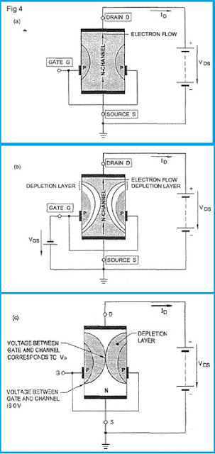
Thus, by varying the reverse bias voltage between gate and source(‐VGS), the drain current can be varied between maximum current (with –VGS=O) and zero j current(with ‐VG,=pinch off voltage). So, JFET can be referred as a voltage controlled devices.
Advantages of FETS:
FETs combine the many advantages of both BJTS and vacuum tubes. Some of their main advantages are;
- High input impedance,
- Small size,
- Ruggedness,
- Long life,
- High frequency response,
- Low noise
- Negative temperature coefficient hence better thermal stability
- High power gain
- A high immunity to radiatility,
- No offset voltage when used as a switch (or copper)
- Square law characteristics.
The only disadvantage are;
- Small gain‐bandwidth product,
- Greater susceptibility to damage in handing them.
APPLICATIONS:‐
- As input amplifiers in oscilloscopes and other electronic testing instruments.
- In logic circuits.
- As ‘mixer’ of FM in TV receivers.
- As VVR (voltage‐variable‐resistor) in operational amplifiers and tone control circuits of audio amplifiers.
- In computers for large scale integration (LSI), in memory circuits.


0 Comments
If you have any doubts, please let me know