
AM Modulators
AM Modulator is one which is used for super imposing allow frequency signal on a high frequency carrier signal .In this modulator the amplitude of a carrier is varied in accordance with instantaneous value of message signal.
- Plate Modulator
- Grid Modulator
- Cathode Modulator
- Base
Modulator
- Emitter Modulator

It is so named because the
message signal (AF) is superimposed on +Vsb and tVsb and then applied to the
plate of a triode tube. Now we will study how modulation occurs in this
modulator.
- The audio voltage (AF) is placed in series with the plate supply voltage +Vbb of a class C amplifier. In actual circuits as shown in figure. How this condition is obtained ? AF signal is applied to the AD driver transformer which varies the grid bias of both triodes in accordance to the message signal. Due to which plate currents of both triodes vary with respect to the frequency of AF signal hence the Voltage +Vbb applied to the plate of class C amplifier vary in accordance to the amplitude of the AF signal.

2. Now we will see that RF (Radio Frequency) is superimposed on the plate voltages (which in
-Ve bias of the grid of class C amplifier is controlled by the RF driver transformer. Due to which plate current, varies in accordance to the RF. In this way, the RF is superimposed on AF and the Amplitude Modulated signal is coupled to the load through the tuned transformer.
Note : RFC Chode is
placed in series with the modulating transformer to protect it from RF Damage.

It is so named because the input signals RF, AF and negative Vc voltages are applied to the grid of class C amplifier.
- The modulating voltage (AF) is in series with the negative bias. The modulating voltage is superimposed on the fixed battery bias. Therefore, the amount of bias is proportional to the amplitude of the modulating signal and varies at a rate equal to the modulating frequency.
- The RF input voltages are superimposed on the total bias.
- The resulting plate flows in pulses, the amplitude of each pulse being proportional to the instantaneous bias and therefore to the instantaneous modulating voltage.
- The application of these pulses to the tuned tank circuit will give amplitude modulation.
The modulator is a linear power amplifier that takes the low level modulating signal and amplifies it to a high power level. The modulating output signal is coupled through modulation transformer T1 to the class C amplifier. The secondary winding of the modulation transformer is connected in series with the collector supply voltage Vcc of the class C amplifier.

With zero modulation input signal. There will be zero modulation voltage across the
secondary of T1. Therefore, the
collector supply voltage
will be applied directly to the class C amplifier, and the output carrier will
be a steady sine wave.
When the modulation signal occurs, the AC voltage across
the secondary of the modulation transformer will be added to and subtracted from the collector supply voltage.
This varying supply voltage is applied to the class C amplifier.
Naturally, the amplitude
of the current pulses through transistor 01 will vary. As a result, the amplitude
of the carriers in e wave
varies in accordance with the
modulated signal. For example, when the modulating signal goes positive, it adds to the collector supply voltage, thereby increasing its value and
causing higher current pulses and a higher amplitude carrier. When the modulating signal goes negative, it subtracts from the collector
supply voltage making it less. For
that reason, the
class C amplifier current pulses are smaller, thereby causing a lower amplitude carrier output.
Hence amplitude modulated wave is
obtained which is then transmitted through antenna.
It is so named because RF carrier and the message signal both are provided to the base of the transistor.
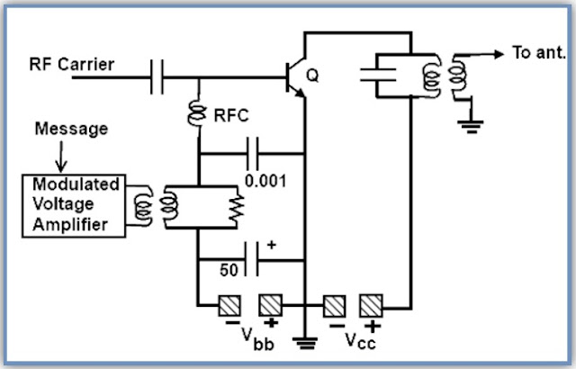
- Message signal is amplified and the n superimposed on the fixed bias Vbb which varies in accordance to the message signal. Then this superimposed bias is provided to the base of the transistor through RFC (Radio Frequency Choke).
- The RF carrier is also provided to the base of the transistor through coupling capacitor which is then superimposed with the message signal bias. This superimposed bias voltages control the collector current which is proportional to the amplitude of the message signal, hence this modulated waveform is coupled to the secondary of the transformer.


0 Comments
If you have any doubts, please let me know