Translate

Search This Blog

Information Technology

ICTSM: The Unseen Force Behind Seamless Operations.

Industrial Visit

Beyond the Classroom, into the Industry. Connecting Theory to the Real World, Where Skills Get Real.

The Blueprint for Success is in Your Hands.

Hands-on Training for a Head-Start Career.

Technology Made Simple

The Expertise to Uncomplicate Your World.

Where Minds and Machines Connect.

Transforming Ideas into Digital Reality.

Saturday, 20 November 2021

PN Junction Diode


The PN junction diode is made up of semiconductor material. It is always conducted in one direction and hence used for rectification. The PN junction diode has two terminals namely anode and cathode. The current flows from anode to cathode.     


The PN junction diode conducts only when it is connected in forward biased. The symbolic representation of PN junction diode is shown in the figure above. The arrow head represents the positive potential, and the bar shows the negative potential of the diode. 


The PN junction diode has a P-type and N-type semiconductor material which is joined by the process of alloying. Thus, both the ends of the diode has different properties. The electrons are the majority charge carrier of the N-type material, and the holes are the majority charge carrier of the p-type semiconductor material. The region in which both the p-type and n-type material meets is known as the depletion region. This region does not have any free electrons because electrons and holes combine with each other in this region.


The depletion region is very thin, and it does not allow the current to flow through it. The PN junction starts conducting when the forward bias is applied across the junction. The forward bias means the P-type material is connected to the positive terminal of the battery and the N-type material is connected to the negative supply.

The forward biased creates the electric field which reduces the depletion region of the PN-junction diode. When the potential barrier is completely reduced, it creates the conducting path for the flow of current. Thus, large current starts flowing, and this current is called the forward current.


Difference Between Forward & Reverse Biasing


Biasing means the electrical supply or potential difference is connected to the semiconductor device. The potential difference is of two types namely – forward bias and the reverse bias.

Basis for Comparison

       Forward Biasing                               

         Reverse Biasing

Definition

The external voltage which is applied across the PN-diode for reducing the potential barrier to constitutes the easy flow of current through it is called forward bias.               

The external voltage which is applied to the PN junction for strengthening the potential barrier and prevents the flow of current through it is called reverse bias.

Symbol

symbol-of-forward-bias

 reverse-bias

Connection        

The positive terminal of the battery is connected to the P-type semiconductor of the device and the negative terminal is connected to N-type semiconductor

The negative terminal of the battery is connected to the P-region and the positive terminal of the battery is connected to N-type semiconductor.


Barrier Potential              

Reduces              

Strengthen

Voltage               

The voltage of an anode is greater than cathode.   

The voltage of cathode is greater than an anode.


Forward Current             

Large    

Small

Depletion layer

Thin      

Thick

Resistance         

Low       

High

 Current Flow    

Allows

Prevents

Magnitude of Current   

Depends on forward voltage.    

Zero

Operate              

Conductor          

Insulator


Theory 24 :- Diode, Symbol, Its Types - Characteristics And Applications

Definition:

A Diode is an electrical device that allows the current to flow in one direction only and shows maximum resistance for the current to flow in the opposite direction. A diode carries two terminals called anode and cathode. The anode is a positive terminal and the cathode is a negative terminal and the current will only flow from the anode terminal to the cathode terminal.

Symbol:

The following figure shows the electrical symbol of the diode.


Working:

The working of the diode depends on the interaction between the P and N junction. The P junction is a region that contains a high concentration of holes while the N junction is a region that contains a high concentration of electrons.

To understand the working of the diode we’ll take three following conditions.
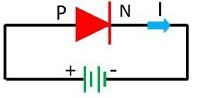
A: Forward Biased Diode:

Forward biased condition will occur when the P-type material of the diode is connected with the positive terminal of the source and the N-type material is connected with the negative terminal of the source.


At first, when we increase the voltage from zero, no current will flow through the diode due to the presence of a potential barrier. However, when the applied voltage exceeds the forward potential barrier, the diode will behave as a short-circuited path and the current flow will be resisted by the external resistors.
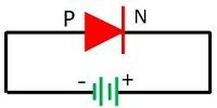
Reverse Biased Diode:

This condition will occur when the P-type material of the diode is connected to the negative terminal of the source and the N-type material is connected to the positive terminal of the source.


In this condition, the holes present in the P region will shift further away from the depletion region due to electrostatic attraction. As a result, more uncovered negative ions will be left behind. In this scenario, there will be no current flow in the circuit.

Unbiased PN-Junction Diode:


In unbiased conditions, there will be no voltage applied from the external energy source. When the P and N junctions are attached, it results in the flow of electrons from the n-type material to the p-type material, and the flow of holes from p-type material to the n-type material.

This flow of charge carriers will generate the third region where no charge carriers are present, this third region is called the depletion region.

Characteristics:


The characteristics of the diodes can be demonstrated by the current-voltage curve. This means, for a certain amount of current we’ll measure the respective voltage across it. The resistors show the linear V-I relationship, however, in the case of diodes this relationship is different. The following figure shows the V-I curve of the diode.

The diode operates in three different regions based on the voltage applied across it.

·     Forward Bias Region: When the positive voltage is applied across the diode, the diode will be turned ON and the current will pass through it. To flow the current through the diode in the forward bias region, the positive voltage should exceed the forward voltage Vf.

·     Reverse Bias Region: In this region, the diode will be turned OFF and the applied voltage will be less than the forward voltage Vf and more than the breakdown voltage Vbr. In this condition, the device shows the maximum resistance for the current, however, a very small amount of current will flow through the diode called reverse saturation current.

·     Breakdown Region: When a very large and negative voltage is applied across the diode, it will allow the current to flow in a reverse direction from cathode to anode. This region is called the breakdown region.

Types:

The diodes are divided into the following different types.

Zener Diodes:

Zener diodes are heavily doped semiconductor devices that conduct in reverse bias conditions. They are also known as reverse breakdown diodes and come with breakdown voltage below 5V. Because of the presence of heavily doped semiconductor material, the Zener diode constitutes a very thin depletion region to increase the electric field intensity.

Photodiodes:

Photodiodes are the right match for solar cells and optical communication applications because they can sense light and are mostly packaged in a material that allows the light to pass through it. A range of photodiodes can be incorporated in a single device either as a two-dimensional array or as a linear array.

Avalanche Diodes:

Avalanche diodes are similar to Zener diodes with one difference i.e. both come with a temperature coefficient of different polarities. These diodes start conducting in the reverse direction when the reverse-biased voltage surpasses the breakdown voltage. At a certain reverse voltage, these diodes break down without being destroyed.

Crystal Diodes:

These diodes are point contact diodes. They contain a semiconductor crystal material for cathode, and the anode is made up of thin metal. These diodes are also called Cat’s Whisker Diode and are not easily available in the market.

LED Diodes:

LED diodes contain a crystalline substance that can emit light in different colours including orange, red, green, and blue, based on the crystalline substance used in the diode. These diodes are widely used in signal applications and are called low-efficiency devices.

PIN Diodes:

PIN diodes are widely used in power electronics because they can bear high voltages. A PIN diode contains a p-type/intrinsic/n-type structure because of an un-doped central layer. They are frequently employed as attenuators and frequency switches.

Applications:

The diodes are used in the following applications.

·     Used as a waveform clipper

·     Used to control the flow of current

·     Incorporated for demodulation of the amplitude signal

·     Employed for temperature measuring applications

·     Used in the construction of rectifiers to convert AC signal to DC signal


Tuesday, 16 November 2021

THEORY- 28 INTRODUCTION TO ZENER DIODE

Zener Diode Zener diode is a P-N junction diode specially designed for operation in the breakdown region when the voltage is above a certain value known as the Zener voltage. Zener diode may be Silicon or Germanium one but Silicon is preferred over Germanium because of higher operating temperature and current capability. The knee point is also sharper in the case of silicon. Zener diode is like an ordinary P-N junction diode except that it is highly doped so as to have a sharp breakdown voltage. These Zener diodes are special diodes which are effectively utilized in the reverse breakdown region. It does not mean that the Zener diode is only operable in the reverse breakdown. It can be used in the forward region also. In the forward characteristic it will be similar to the VI characteristic of normal diode. The Zener diode is manufactured with adequate power dissipation capabilities so that they can operate in the breakdown region. Normal diodes cannot operate in breakdown region because normal diodes do not have the high power dissipation capability. That is why it is dangerous to use a normal diode in the breakdown region. But the Zener diode has higher power dissipation capability so that they can be used in the breakdown region without any danger of degrading their properties. The voltage drop across the Zener diode is equal to the Zener voltage of that diode no matter how high the reverse bias voltage is above the Zener voltage.


The illustration above shows this phenomenon in a Current vs. Voltage graph. With a zener diode connected in the forward direction, it behaves exactly the same as a standard diode – i.e. a small voltage drop of 0.3 to 0.7V with current flowing through pretty much unrestricted. In the reverse direction however there is a very small leakage current between 0V and the Zener voltage – i.e. just a tiny amount of current is able to flow. Then, when the voltage reaches the breakdown voltage (Vz), suddenly current can flow freely through it. For example if you pass a reverse 5V through a 3V zener diode and measure the voltage across the zener diode, that voltage will be 3V.


Zener Diode as a Voltage Regulator 

Since the voltage dropped across a Zener Diode is a known and fixed value, Zener diodes are typically used to regulate the voltage in electronic circuits. A zener diode can be used to make a simple voltage regulation circuit as shown in figure. The output voltage is fixed as the zener voltage of the zener diode used and so can be used to power devices requiring a fixed voltage of a certain value (equal to the rating of the zener diode).


Case 1: Load resistance is constant and input voltage is varying


·         Load resistance is constant means load current (IL) will also be constant as VL = VZ is constant.

·         Now if we increase the input voltage (Vin), current IS will increase. Due to which zener current IZ will increase as IL is constant.

·         But the maximum current which can pass through the zener is Iz(max). Therefore, there will· be a limit up to which we can increase the input voltage so that zener current will remain below Iz(max) and it will define the maximum limit of input voltage (Vin(max)) for successful operation as voltage regulator.

·         Now if we decrease the input voltage (Vin), current IS will decrease. Due to which zener current IZ will decrease as IL is constant.

·         But the minimum current which can pass through the zener is Iz(min). Therefore, there will be a limit up to which we can decrease the input voltage so that zener current will remain above Iz(min) and it will define the minimum limit of input voltage (Vin(min)) for successful operation as voltage regulator.

·         To maintain a constant voltage at output, input voltage Vin will have the following limit Vin(min) < Vin < Vin (max).

·         This limit is based on Iz(min) and Iz(max) which is the limit of current that can pass through the zener while maintaining the constant zener voltage VZ.

Case 2: Input voltage is constant and load resistance is varying


Input voltage is constant means current IS will also be constant.  

Now if we increase the load resistance (RL), load current IL will decrease as V= = VZ is· constant. Due to which zener current IZ will increase as IS is constant.

But the maximum current which can pass through the zener is Iz(max). Therefore, there will be a limit up to which we can increase the load resistance so that zener current will remain below Iz(max) and it will define the maximum limit of load resistance (RL(max)) for successful operation as voltage regulator.

Now if we decrease the load resistance (RL), load current IL will increase as VL = VZ is constant. Due to which zener current IZ will decrease as IS is constant.

But the minimum current which can pass through the zener is Iz(min). Therefore, there will be a limit up to which we can decrease the load resistance so that zener current will remain above Iz(min) and it will define the minimum limit of load resistance (RL(min)) for successful operation as voltage regulator.

To maintain a constant voltage at output, load resistance RL will have the following limit RL(min) < RL < RL(max)  

This limit is based on Iz(min) and Iz(max) which is the limit of current that can pass through the zener while maintaining the constant zener voltage VZ.


Theory 23 :- Types of Semiconductors


Types of Semiconductors

Semiconductors are mainly classified into two categories:

1. Intrinsic Semiconductor

2. Extrinsic Semiconductor


Intrinsic Semiconductor An intrinsic semiconductor material is chemically very pure and possesses poor conductivity. It has equal numbers of negative carriers (electrons) and positive carriers (holes).

Extrinsic Semiconductor Where as an extrinsic semiconductor is an improved intrinsic semiconductor with a small amount of impurities added by a process, known as doping, which alters the electrical properties of the semiconductor and improves its conductivity. Depending on whether the added impurities have “extra” electrons or “missing” electrons determines how the bonding in the crystal lattice is affected as shown in figure, and therefore how the material’s electrical properties change.


The Doping of Semiconductors

The addition of a small percentage of impurity atoms in the intrinsic semiconductor (pure silicon or pure germanium) produces dramatic changes in their electrical properties. Depending on the type of impurity added, the extrinsic semiconductors can be divided in to two classes:

 1. N-type Semiconductors

2. P-type Semiconductor


N-Type Semiconductor

Group V dopants are the atoms with an “extra” electron, in other words a valence shell with only one electron. When a semiconductor is doped with a Group V impurity it is called an n-type material, because the addition of these pentavalent impurities such as antimony, arsenic or phosphorous contributes free electrons, greatly increasing the conductivity of the intrinsic semiconductor. In an n-type semiconductor, the majority carrier, or the more abundant charge carrier, is the electron, and the minority carrier, or the less abundant charge carrier, is the hole.

The effect of this doping process on the relative conductivity can be explained by energy band diagram shown in figure. When donor impurities are added to an intrinsic semiconductor, allowable energy levels are introduced at a very small gap below the conduction band, as illustrated in figure. These new allowable levels are essentially a discrete level because the added impurity atoms are far apart in the crystal structure and hence their interaction is small. In the case of Silicon, the gap of the new discrete allowable energy level is only 0.05 eV (0.01 eV for germanium) below the conduction band, and therefore at room temperature almost all of the "fifth" electrons of the donor impurity are raised into the conduction band and the conductivity of the material increases considerable.


P-Type Semiconductor

Group III dopants are the atoms with a hole in their valence shell (only “missing” one electron), When a semiconductor is doped with a Group III impurity it is called a p-type material, The addition of these trivalent impurities such as boron, aluminum or gallium to an intrinsic semiconductor creates deficiencies of valence electrons, called "holes". In an p-type semiconductor, the majority carrier, or the more abundant charge carrier, is the hole, and the minority carrier, or the less abundant charge carrier, is the electron. The effect of this doping process on the relative conductivity can be explained by energy band diagram shown in figure. When accepter impurities or P type impurities are added to the intrinsic semiconductor, they produce an allowable discrete energy levels which is just above the valance band, as shown in figure. Since a very small amount of energy (0.08 eV in case of Silicon and 0.01 eV in case of Germanium) is required for an electron to leave the valence band and occupy the accepter energy level, holes are created in the valence band by these electrons.