.jpeg)


Filter Circuits
The filter circuit can be constructed by the combination of components like capacitors, resistors, and inductors. Inductor is used for its property that it allows only dc components to pass and blocks ac signals. Capacitor is used so as to block the dc and allows ac to pass. All the combinations and their working are explained in detail below.

Series
Inductor Filter
The
circuit diagram of a full wave rectifier with a series inductor filter is given
below.

As the name of the filter circuit suggests, the Inductor L is connected in series between the rectifier circuit and the load. The inductor carries the property of opposing the change in current that flows through it.
In
other words, the inductor offers high impedance to the ripples and no impedance
to the desired dc components. Thus the ripple components will be eliminated.
When the rectifier output current increases above a certain value, energy is
stored in it in the form of a magnetic field and this energy is given up when
the output current falls below the average value. Thus all the sudden changes in
current that occurs in the circuit will be smoothened by placing the inductor
in series between the rectifier and the load.
The
waveform below shows the use of inductor in the circuit.
From
the circuit, for zero frequency dc voltage, the choke resistance Ri in series
with the load resistance RL forms a voltage divider circuit, and thus the dc
voltage across the load is
Vdc =
RL/(Ri + RL)
Vdc is the output from a full wave rectifier. In this case, the value of Ri is negligibly small when compared to RL.
The
effect of higher harmonic voltages can be easily neglected as better filtering
for the higher harmonic components take place. This is because of the fact that
with the increase in frequency, the reactance of the inductor also increases.
It should be noted that a decrease in the value of load resistance or an
increase in the value of load current will decrease the amount of ripples in
the circuit. So, the series inductor filter is mostly used in cases of high
load current or small load resistance. A simple series inductor filter may not
be properly used. It is always better to use a shunt capacitor (C) with series
inductor (L) to form an LC Filter.
Shunt Capacitor Filter
As
the name suggests, a capacitor is used as the filter and this high value
capacitor is shunted or placed across the load impedance. This capacitor, when
placed across a rectifier gets charged and stores the charged energy during the
conduction period. When the rectifier is not conducting, this energy charged by
the capacitor is delivered back to the load. Through this energy storage and
delivery process, the time duration during which the current flows through the
load resistor gets increased and the ripples are decreased by a great amount.
Thus for the ripple component with a frequency of ‘f’ megahertz, the capacitor
‘C’ will offer a very low impedance. The value of this impedance can be written
as:
Shunt Capacitor Impedance = 1/2 fC
Thus the dc components of the input signal along with the
few residual ripple components, is only allowed to go through the load
resistance RLoad. The high amount of ripple components of current gets bypassed
through the capacitor C.
Now
let us look at the working of Half-wave rectifier and Full-wave rectifier with
Capacitor filters, their output filtered waveform, ripple factor, merits and
demerits in detail.
2.1 Half-wave Rectifier with Capacitor Filter

The circuit diagram above shows a half-wave rectifier
with a capacitor filter. The filter is applied across the load RLoad. The
output of the RLoad is VLoad, the current through it is ILoad. The current
through the capacitor is Ic.
During
the positive half cycle of the input ac voltage, the diode D will be forward
biased and thus starts conducting. During this period, the capacitor ‘C’ starts
charging to the maximum value of the supply voltage Vsm. When the capacitor is
fully charged, it holds the charge until the input ac supply to the rectifier
reaches the negative half cycle. As soon as the negative half supply is
reached, the diode gets reverse biased and thus stops conducting. During the
non-conducting period, the capacitor ‘C’ discharges all the stored charges
through the output load resistance RLoad. As the voltage across RLoad and the
voltage across the capacitor ‘C’ are the same (VLoad = Vc), they decrease
exponentially with a time constant (C*RLoad) along the curve of the
non-conducting period. This is shown in the graph below.

The value of the discharge time constant (C*RLoad) being
very large, the capacitor ‘C’ will not have enough time to discharge properly.
As soon as the capacitor starts discharging, the time becomes over. Thus the
value of RLoad at the discharge time will also be high and have just a little
less value that the output of RLoad. This is when the positive half cycle
repeats again and the diode starts conducting. The condition to be considered
at this stage is that the rectified voltage takes value more than the capacitor
voltage . When the condition occurs the capacitor starts charging to a value of
Vsm. The condition again changes when the negative half cycle comes into pace,
and the whole cycle is again repeated to form the output waveform as shown
above. The output shows a nearly constant dc voltage at the load and that the
output voltage is increased considerably.
Thus,
in short:
· If
the value of load resistance is large, the discharge time constant will be of a
high value, and thus the capacitors’ time to discharge will get over soon. This
lowers the amount of ripples in the output and increases the output voltage. If
the load resistance is small, the discharge time constant will be less, and the
ripples will be more with decrease in output voltage.
· The
value of the capacitor used plays an important role in determining the output
ripples and the average dc level. If the capacitor value is high, the amount of
charge it can store will be high and the amount it discharges will be less.
Thus the ripples will be less and the average dc level will be high. But, there
is a limit on how much capacitance can b increased. If the capacitor value is
increased to a very high value, the amount of current required to charge the
capacitor to a given voltage will be high. This value of current depends on the
manufacturer of the diode and will be surely limited to a certain value. Thus,
there is a limit in increasing the capacitor value in a half-wave rectifier
shunt capacitor filter circuit.
·
Poor
voltage regulation.
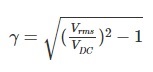
Ripple
Factor
The
rms value depends on the peak value of charging and discharging magnitude,
Vpeak.
Vac
rms = Vpeak/2
Vpeak
= Idc/fC
Ripple Factor = Vac rms/Vdc = (Vpeak/2 ) * (1/Idc.RLoad)
= Idc/(2
.Idc.RLoad.f.C) = 1/(2 fCRLoad)
2.2 Full-wave Rectifier with
Shunt Capacitor Filter
The
circuit diagram of a full-wave rectifier wit capacitor filter is shown below.

The
filter capacitor C is placed across the resistance load RLoad. The whole
working is pretty much similar to that of a half-wave rectifier with shunt
capacitor explained above. The only difference is that two pulses of current
will charge the capacitor during alternate positive (D1) and negative (D2) half
cycles. Similarly capacitor C discharges twice through RLoad during one full
cycle. This is shown in the waveform below.

The load current reduces by a smaller amount before the
next pulse is received as there are 2 current pulses per cycle. This causes a good
reduction in ripples and a further increase in the average dc load current.
L-C Filters
In the simple shunt capacitor
filter circuit explained above, we have concluded that the capacitor will
reduce the ripple voltage, but causes the diode current to increase .This large
current may damage the diode and will further cause heating problem and decrease
the efficiency of the filter. On the other hand, a simple series inductor
reduces both the peak and effective values of the output current and output
voltage. Then if we combine both the filter (L and C), a new filter called the
L-C filter can be designed which will have a good efficiency, with restricted
diode current and enough ripple removal factor .The voltage stabilizing action
of shunt capacitor and the current smoothing action of series inductor filter
can be combined to form a perfect practical filter circuit.
L-C
filters can be of two types: Choke Input L-section Filter and L-C Capacitor
input filter
Choke Input L-Section Filter
An
inductor filter increases the ripple factor with the increase in load current
Rload. A capacitor filter has an inversely proportional ripple factor with
respect to load resistance. Economically, both inductor filter and capacitor
filter are not suitable for high end purpose
L-C
inductor input or L-section filter consists of an inductor ‘ L’ connected in
series with a half or full wave rectifier and a capacitor ’C’ across the load.
This arrangement is also called a choke input filter or L-section filter
because it’s shape resembles and inverted L-shape. To increase the smoothing
action using the filter circuit, just one L-C circuit will not be enough.
Several L-section filters will be arranged to obtain a smooth filtered output.
The circuit diagram and smoothened waveform of a Full wave rectifier output is
shown below.
Choke Input L-Section Filter
An
inductor filter increases the ripple factor with the increase in load current
Rload. A capacitor filter has an inversely proportional ripple factor with
respect to load resistance. Economically, both inductor filter and capacitor
filter are not suitable for high end purpose
L-C inductor input or L-section filter consists of an inductor ‘ L’ connected in series with a half or full wave rectifier and a capacitor ’C’ across the load. This arrangement is also called a choke input filter or L-section filter because it’s shape resembles and inverted L-shape. To increase the smoothing action using the filter circuit, just one L-C circuit will not be enough. Several L-section filters will be arranged to obtain a smooth filtered output. The circuit diagram and smoothened waveform of a Full wave rectifier output is shown below.

As shown in the circuit diagram above, the inductor L allows the dc to pass but restricts the flow of ac components as its dc resistance is very small and ac impedance is large. After a signal passes through the choke, if there is any fluctuation remaining the current, it will be fully bypassed before it reaches the load by the shunt capacitor because the value of Xc is much smaller than Rload. The number of ripples can be reduced to a great amount by making the value of XL greater than Xc at ripple frequency.
Ripple Factor
Ripple Factor = Vac rms/Vdc = (√2/3)(Xc/XL) = (√2/3)(1/[2wc])(1/[2wL]) = 1/(6√2w2LC)
Though the L-C filter has all these advantages, it has now become quite obsolete due the huge size of inductors and its cost of manufacturing. Nowadays, IC voltage regulators are more commonly used along with active filters, that reduce the ripples and keeps the output dc voltage constant.
The diagram of L-C Capacitor input filter and waveform is shown below.
Π – Filter or Capacitance Input Filter
The
name pi – Filter implies to the resemblance of the circuit to a Π shape with
two shunt capacitances (C1 and C2) and an inductance filter ‘L’. As the
rectifier output is provided directly into the capacitor it also called a
capacitor input filter.
he output from
the rectifier is first given to the shunt capacitor C. The rectifier used can
be half or full wave and the capacitors are usually electrolytic even though
they large in size. In practical applications, the two capacitances are
enclosed in a metal container which acts as a common ground for the two
capacitors. Circuit diagram and the waveform are given below.

When compared
to other type of filters, the Π – Filter has some advantages like higher dc
voltage and smaller ripple factor. But it also has some disadvantages
like poor voltage regulation, high peak diode current, and high peak inverse
voltage.
This filter is
divided into two – a capacitor filter and a L-section filter. The capacitor C1
does most of the filtering in the circuit and the remaining ripple os removed
by the L-section filter (L-C2). C1 is selected to provide very low reactance to
the ripple frequency. The voltage regulation is poor for this circuit as the
output voltage falls off rapidly with the increase in load current.
Ripple Factor
Ripple Factor = √2/(8w3C1C2LRload)
R-C Filter
We have already
discussed about the drawbacks of using a pi-filter. The main reason for all
these drawbacks is the use of inductor in the filter circuit. If we use a
resistance in series, instead of the inductor as the filter, these drawbacks
can be overcome. Thus the circuit is named as R-C filter. In this circuit, the
ripples have to be made to drop across the resistance R instead of the load
resistance RL. For this, the value of RL is kept much larger than the value of
reactance of capacitor C2 (XC2). This means that each section reduces the
ripple by a factor of at least 10.

Though the
circuit nullifies certain drawbacks of the pi-filter, the circuit on its own
has some problems as well. The filter has very poor voltage regulation. There
is a large voltage drop in the resistance R. The circuit also develops a lot of
heat and this has to be dissipated through enough and adequate ventilation.
Thus, the filter is only suitable for small load current or large load resistance
circuits.